
Market Minds Advisory
Advanced Packaging Market

Advanced Packaging Market: Interposer Capacity as the New Chokepoint.

AI accelerator makers now design chips around available packaging capacity rather than the reverse, chiplet architectures push monolithic die design toward obsolescence, and assembly houses without qualified interposer lines lose the largest datacenter contracts outright.

Lead Analyst

Bilal Shaikh

Published

August 2026

Make Smarter Decisions with Customized Research Insights

Request a free sample report and evaluate market opportunities, growth trends, and competitive dynamics relevant to your business needs.

2025 MARKET VALUE$48.0BMarket Size 2025
2036 FORECAST VALUE$148.3BBase Case , 2026 to 2036
CAGR 2026 TO 203610.8 %Bull 12.1% / Bear 9.5%
INCREMENTAL OPPORTUNITY$95.1BNet 10- year value creation
EXPANSION MULTIPLE2.79x2036 value over 2026 base
Strategic Levers
M&A Pipeline
Regional Outlook
Country Rankings
Competitive Intelligence
Segmental Deep-dive
Call-Us : 91 93563 13602

Executive Snapshot and Market Trajectory

Chipmakers increasingly treat advanced packaging capacity as the binding constraint on product roadmaps rather than a downstream assembly step, since interposer and high-bandwidth memory integration now determine shipment volume more directly than wafer fabrication capacity itself for the highest-value accelerator products entering production today across every major design house.
2.5D and interposer packaging leads growth at 18.5%, roughly 1.71 times the overall rate, as AI accelerator makers integrate multiple compute and memory dies into single packages that monolithic designs cannot match on bandwidth or power efficiency. East Asia now holds the largest regional share at 30%, driven by Taiwan and South Korea's concentrated advanced packaging manufacturing capacity and proximity to leading foundry operations concentrated within the same regional supply corridors.
Competitive intensity runs high at 64% held by five suppliers, since interposer qualification and chip-on-wafer-on-substrate capacity require enormous capital investment that concentrates share around a handful of established assembly houses rather than fragmenting across regional specialists the way simpler packaging categories often do. Buyers increasingly select suppliers on demonstrated yield and delivery reliability rather than unit price alone across most large-scale supply agreements and multi-year capacity commitments.
Market Definition
Base Year Value
$48.0B in 2025 (MMA Primary Research Dataset, August 2026)
Forecast Period
2026 to 2036, eleven discrete annual values
CAGR
10.8% base case. Bull 12.1%. Bear 9.5%.
Fastest Growth Segment
2.5D and Interposer Packaging: 18.5% CAGR
Fastest Growth Country
South Korea: 13.8% CAGR
Fastest Growth Region
South Asia and Pacific: 12.9% CAGR
Largest Region
East Asia: 30% of 2025 global value
Market Leaders
Primary Survey
n=3,800 procurement and R&D decision-makers, Q4 2025, six countries
Methodology
Demand-side build-up, cross-validated against public data, 47 expert interviews

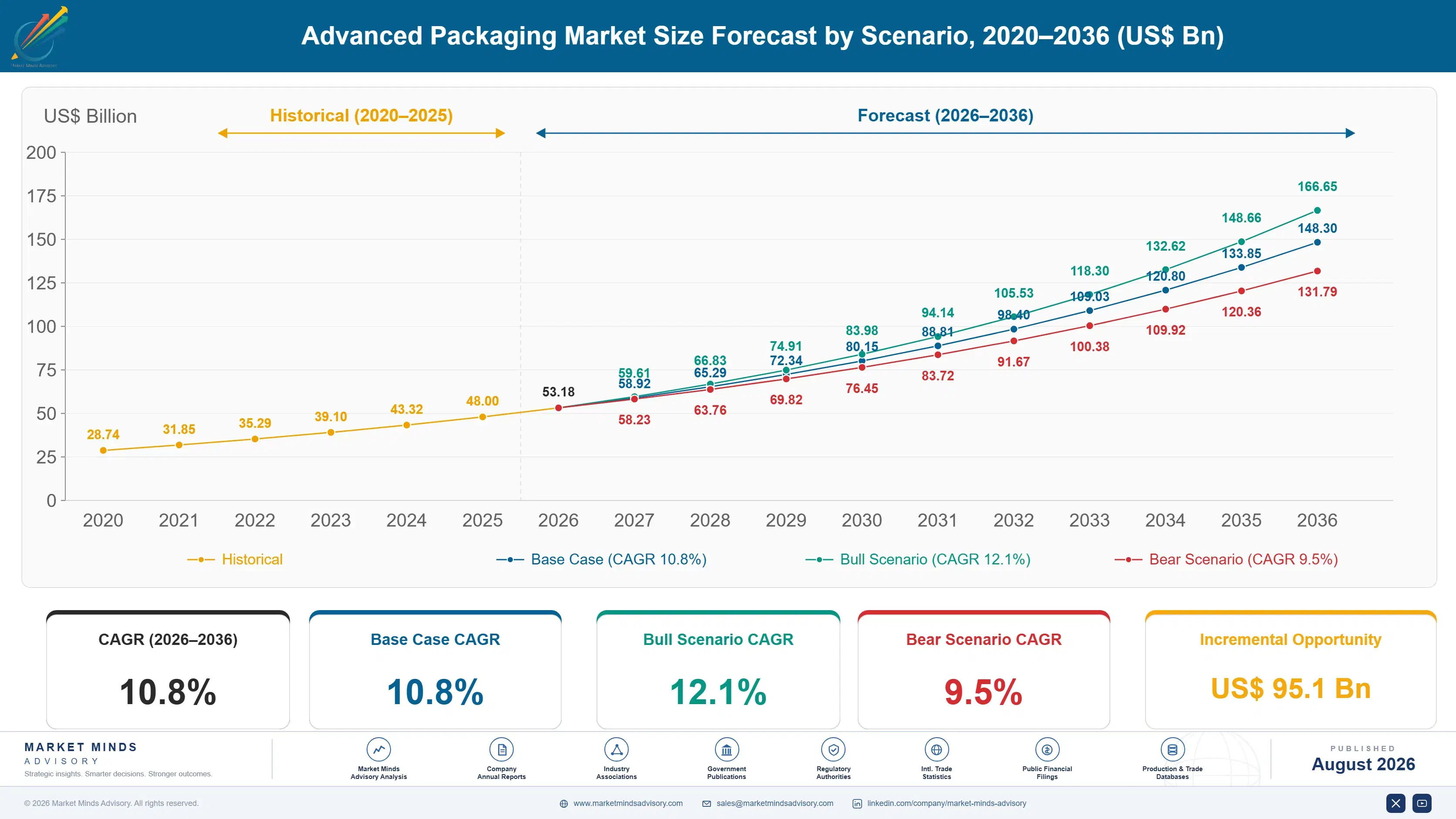
Advanced Packaging Market Forecast Scenarios

advanced-packaging-market-size-forecast-scenario-1787301104265
Between 2020 and 2025 the market grew at an estimated 9.4% annually, accelerating sharply after 2022 as AI accelerator demand pulled advanced packaging from a specialty niche into the central bottleneck constraining the entire semiconductor supply chain worldwide, forcing suppliers to accelerate capacity investment plans considerably faster than originally planned across the industry's largest suppliers.
Three mechanisms carry the base case to 10.8%. First, AI accelerator makers keep integrating more compute and memory dies per package as model complexity grows, expanding the addressable packaging content per chip sold. Second, chiplet architectures are displacing monolithic die design across an expanding range of applications beyond AI accelerators alone. Third, foundries and assembly houses keep expanding packaging capacity, relieving supply constraints that previously capped shipment volume across most product categories.
The bull case at 12.1% assumes sustained AI infrastructure investment keeps packaging demand ahead of capacity expansion timelines currently planned by major suppliers across the industry. The bear case at 9.5% assumes capacity expansion outpaces demand growth as new packaging lines commissioned during the current investment cycle come fully online across multiple producing regions simultaneously through the back half of the decade.

Interposer Capacity as the Real Constraint

Advanced packaging sits at the center of compute economics for any chipmaker pursuing multi-die architectures, since interposer and substrate capacity increasingly determine shipment volume more directly than transistor design or wafer fabrication capability alone. Yield consistency, not raw process innovation, increasingly separates competing suppliers across major procurement decisions and multi-year allocation agreements spanning several product generations.
MARKET CONCENTRATION (CR5)64%Five suppliers hold dominant share across capital-intensive assembly segment
AVERAGE PACKAGE YIELD85 to 93 percentTypical qualified yield rate for advanced interposer assembly processes
TOP PRODUCING COUNTRY SHARE38%Taiwan supplies largest share of installed advanced packaging capacity
CAPACITY BUILDOUT CYCLE18 to 24 monthsTypical timeline from investment decision to qualified production output
SUBSTRATE COST SHARE25-32% of COGSOrganic substrate and interposer materials weigh heavily on costs
TRADE INTENSITY48% cross-borderPackaged components frequently cross borders before final system integration
Commercially, the category behaves like a specialized capital-intensive manufacturing business wrapped inside a broader semiconductor supply chain relationship. Suppliers commit multi-year capacity agreements with major fabless customers well before production lines are even commissioned, which locks buyers into specific assembly partners across an entire product generation rather than encouraging spot-market shopping on price. Switching partners requires costly requalification against yield, reliability, and thermal performance standards across the entire product line.
Over the next decade, expect chiplet-based architectures to keep displacing monolithic die design across an expanding range of applications beyond AI accelerators, as standardized interconnect protocols mature and packaging cost per transistor keeps falling across most product categories. Panel-level packaging will also gain share over traditional wafer-level approaches as suppliers seek greater manufacturing efficiency at scale across their broader production networks.
"The chip design was never the bottleneck. Getting it stacked, wired, and yielding at volume was always the hard part, and now everyone finally admits it."
Director, Semiconductor Manufacturing and Assembly Practice · MMA Technology / S

Market Trends

Chip-on-Wafer-on-Substrate Capacity Becomes a Strategic Asset

TSMC's CoWoS packaging technology has become the single most sought-after manufacturing capability in the semiconductor industry, with customers reportedly committing capital years in advance to secure allocation for future accelerator generations. TSMC has disclosed multi-billion dollar capital expenditure specifically targeting CoWoS capacity expansion, citing sustained demand from AI accelerator customers outpacing even aggressive capacity growth plans. Samsung and Intel have both accelerated competing interposer packaging programs to capture overflow demand that TSMC capacity constraints leave unaddressed. The shift has turned packaging capacity itself into a strategic asset comparable to leading-edge wafer fabrication capability.
Market Impact: Adds 45% packaging content per chip
Chiplet Interconnect Standardization Accelerates Multi-Vendor Design

Industry consortiums including the Universal Chiplet Interconnect Express standard have published specifications enabling chiplets from different vendors to interoperate within a single package, reducing the vertical integration previously required to pursue multi-die architectures. AMD and Intel have both publicly committed to standardized chiplet interfaces across upcoming product generations, signaling confidence that interoperability will not compromise performance versus proprietary interconnect approaches used previously. That standardization is lowering the barrier for smaller design houses to participate in multi-die architectures without building complete in-house packaging expertise from scratch, an increasingly important competitive consideration industry-wide.
Market Impact: Adds 25 new chiplet product lines

Market Opportunities and Growth Drivers

AI Accelerator Complexity Expands Packaging Content Per Chip

Each new generation of AI accelerators integrates more compute dies, more high-bandwidth memory stacks, and more sophisticated interposer routing than its predecessor, expanding the addressable packaging revenue per chip sold well beyond what simple unit volume growth alone would suggest. NVIDIA's flagship accelerators now integrate multiple compute dies alongside numerous memory stacks within a single package, a configuration that would have been considered impractical just several years earlier. That escalating complexity means packaging revenue grows faster than chip unit shipments, since each individual unit carries substantially more packaging content and correspondingly higher assembly value than earlier chip generations.
Market Impact: Requires 3-5 billion per line

Chiplet Adoption Expands Beyond AI Into Mainstream Computing

Chiplet-based design is expanding beyond AI accelerators into mainstream server processors, consumer computing, and networking silicon, as the economic benefits of combining smaller, higher-yielding dies into a single package apply broadly across the semiconductor industry rather than only to the most advanced accelerators. AMD's server processor line has demonstrated chiplet economics at meaningful commercial scale for several years, providing a proven template other chipmakers are now following. Each new chiplet-based product category adds incremental advanced packaging demand independent of AI-specific capital spending cycles, broadening the market's underlying demand base considerably.
Market Impact: Cuts yield 8-15 points

Market Restraints and Challenges

Capital Intensity Limits New Entrant Participation

Building qualified advanced packaging capacity requires capital investment measured in billions of dollars per production line, creating a barrier that effectively excludes all but the largest, best-capitalized suppliers from meaningful participation in the highest-value segments of the market. The root cause is process complexity: interposer and chip-on-wafer-on-substrate assembly demands equipment and clean room infrastructure comparable to leading-edge wafer fabrication rather than traditional lower-cost packaging processes. That barrier concentrates the highest-margin segment among a handful of suppliers regardless of how much technical innovation smaller competitors might otherwise offer. Suppliers are responding by pursuing joint ventures and government-subsidized capacity expansion programs.
Market Impact: Adds 150% CoWoS capacity by 2027

Yield Challenges Persist at Leading-Edge Complexity Levels

Advanced packaging processes involving multiple dies and complex interposer routing face meaningfully lower yield rates than mature, simpler packaging approaches, and a single defective die can compromise an entire expensive multi-die assembly. The root cause is cumulative complexity: each additional die and interconnect layer multiplies the probability of a yield-limiting defect somewhere across the assembly, unlike simpler single-die packages with fewer potential failure points. That yield gap raises effective cost per good unit meaningfully above nameplate process cost, squeezing margin until suppliers mature their process recipes. Suppliers are responding with improved known-good-die testing before committing dies to expensive assembly.
Market Impact: Expands multi-vendor designs 40%
3 additional market trends, 4 additional growth drivers, and 2 additional restraints and challenges are covered in the full report. Contact sales@marketmindsadvisory.com to access the complete intelligence.

Segment CAGR and Growth Architecture

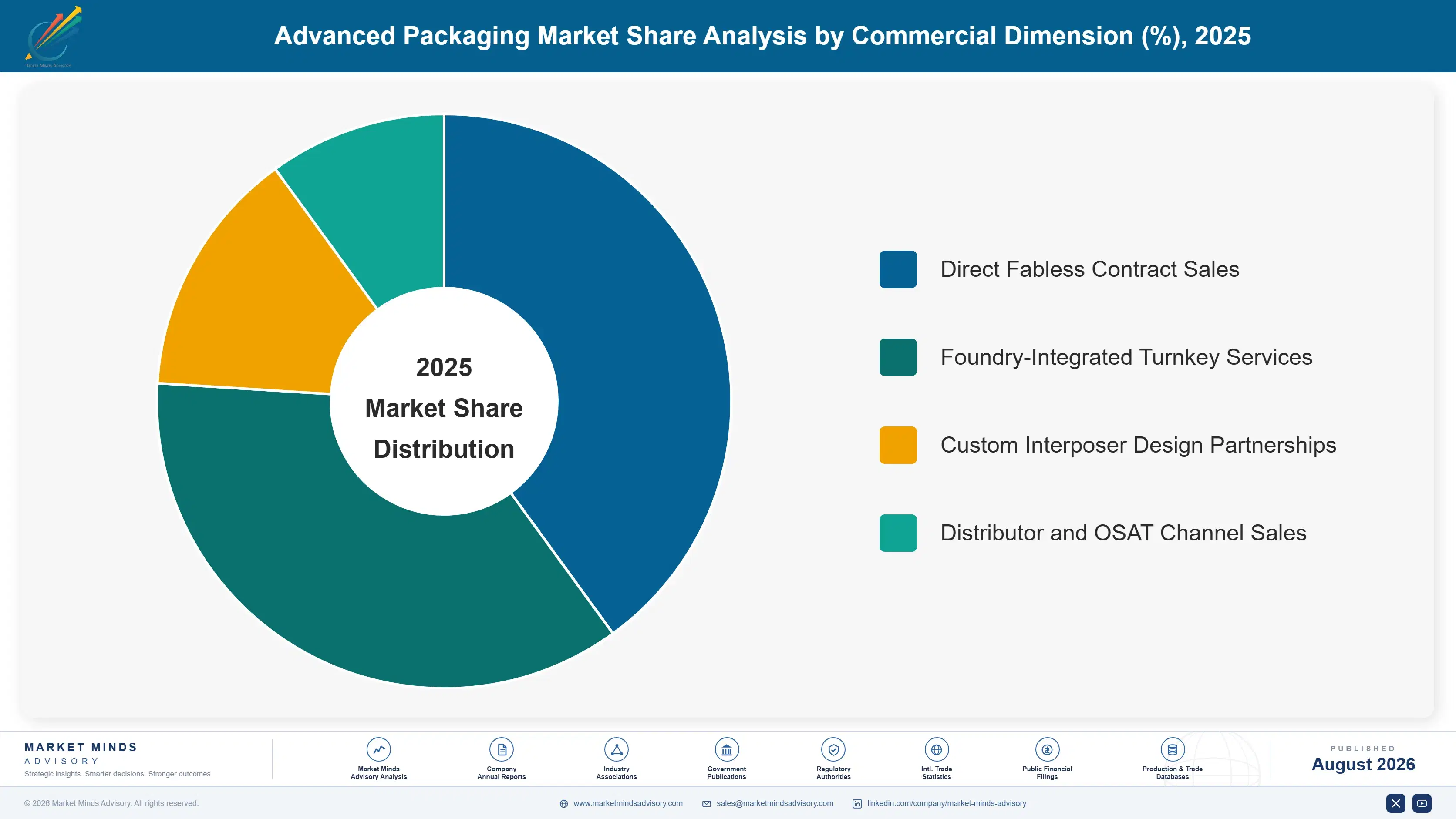
Segmentation follows packaging technology type, a single interconnect-architecture logic spanning 2.5D and interposer, 3D stacked die, fan-out wafer-level, flip chip, system-in-package, and wafer-level chip-scale packaging. Each technology carries distinct process complexity, capital intensity, and application fit, so commercial position tracks the interconnect architecture rather than the specific chip or application it ultimately happens to package.
advanced-packaging-market-market-share-analysis-1787301104840

2.5D and Interposer Packaging

2.5D and interposer packaging grows fastest at 18.5%, about 1.71 times the overall market rate, as AI accelerator makers integrate multiple compute dies alongside numerous high-bandwidth memory stacks within single packages that monolithic designs simply cannot match on bandwidth or power efficiency. Each new accelerator generation demands more interposer routing complexity than its predecessor, expanding addressable packaging content per chip well beyond what unit volume growth alone would suggest. TSMC's CoWoS technology dominates this category commercially, and customers reportedly commit capital years in advance to secure future allocation given how severely constrained current capacity remains relative to accelerator demand across the entire industry's expanding customer base and its multi-year order backlog.
CAGR 18.5%

3D Stacked Die Packaging

3D stacked die packaging grows second-fastest at 15.0%, driven by through-silicon-via technology that enables vertical die stacking for memory-intensive applications where interposer-based lateral integration cannot achieve comparable density within available package footprint. High-bandwidth memory manufacturers, including SK Hynix and Samsung, have both scaled 3D stacking capacity considerably to meet surging demand from AI accelerator customers requiring ever-taller memory stacks per package and higher data transfer bandwidth. The technology's thermal management challenges grow more acute with each additional stacked layer, driving sustained innovation investment in cooling and interconnect reliability across the supplier base and its academic and industrial research partners worldwide, from university cleanroom labs to commercial-scale, high-volume production facilities globally.
CAGR 15.0%
Full segment breakdown across 6 segments available in the complete report.

Regional Architecture and Country Demand Map

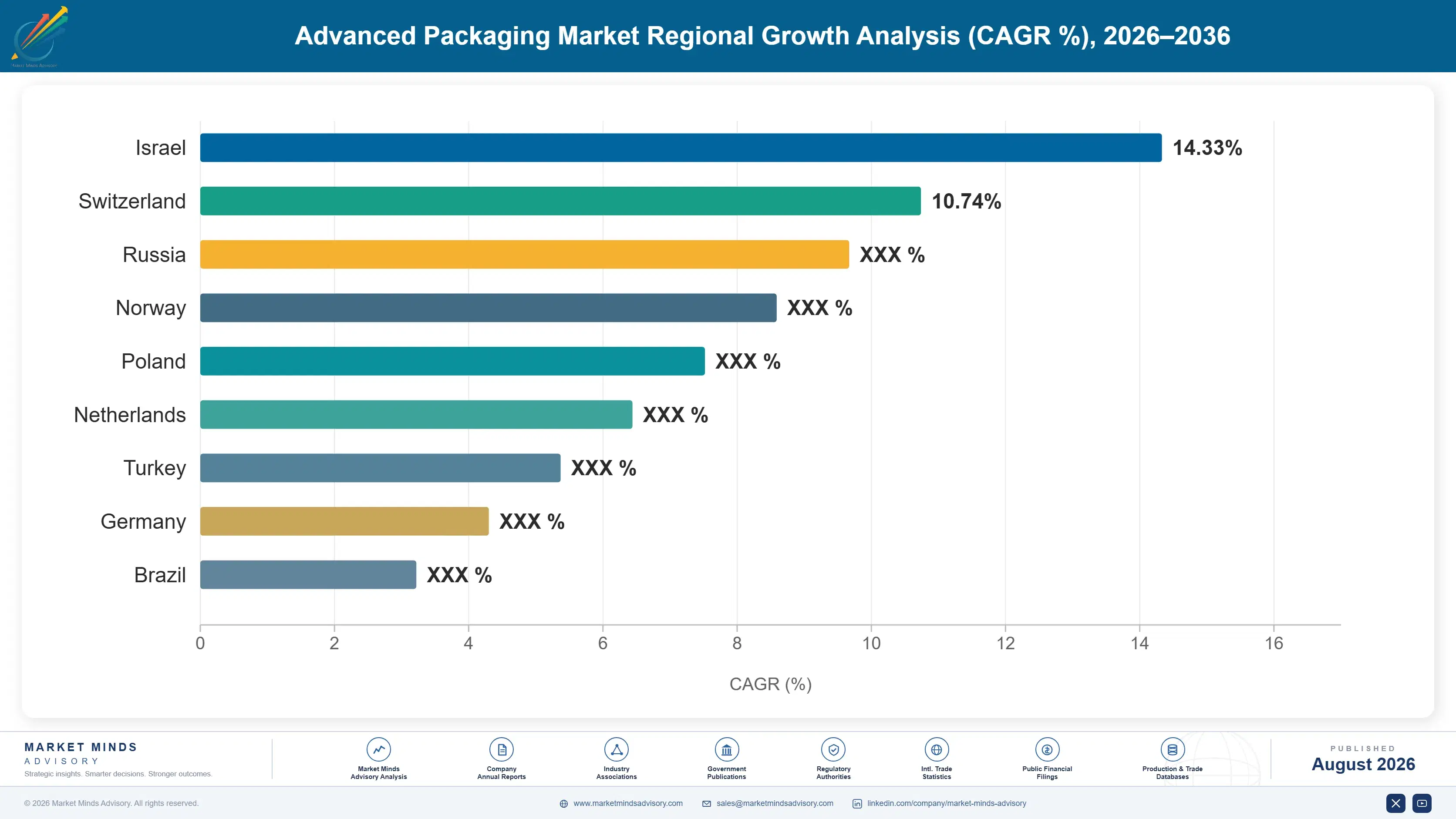
East Asia leads at 30% of global value on Taiwan and South Korea's concentrated packaging manufacturing capacity, followed by North America at 26% and Western Europe at 18% on enterprise chip design demand. Remaining regions together account for the balance of overall global demand today.

North America

United States fabless chip designers anchor North American demand, since NVIDIA, AMD, Broadcom, and Apple all design their most advanced products domestically even though the actual packaging assembly happens predominantly overseas at qualified Asian facilities. American onshoring incentives under the CHIPS Act have begun attracting advanced packaging investment domestically, though qualified capacity remains a small fraction of Asian production at present. Intel maintains substantial domestic advanced packaging capacity supporting both its own advanced products and foundry customers seeking geographic diversification away from concentrated Asian supply. Growth of 11.5% outpaces the global rate as AI accelerator design activity and onshoring investment compound across the region's expanding semiconductor design and manufacturing base.
Share: 26% | CAGR: 11.5% (2026 to 2036)

Western Europe

Germany hosts meaningful semiconductor equipment and materials supply chain activity supporting advanced packaging processes globally, even though the region's direct packaging assembly capacity remains genuinely limited compared with Asian manufacturing hubs. The Netherlands anchors critical equipment supply through ASML and BE Semiconductor Industries, both essential suppliers to advanced packaging processes worldwide, regardless of where final assembly ultimately occurs geographically. France and the United Kingdom contribute meaningful chip design activity that ultimately still depends heavily on Asian packaging capacity for final production and assembly. Growth of 9.3% trails the global average because the region's role concentrates in upstream equipment and materials rather than downstream assembly capacity itself, which remains concentrated elsewhere.
Share: 18% | CAGR: 9.3% (2026 to 2036)
Regional intelligence for 5 additional markets available in the complete report: East Asia, South Asia and Pacific, Latin America, Middle East and Africa, Eastern Europe. Contact sales@marketmindsadvisory.com.
advanced-packaging-market-country-cagr-analysis-1787301105350

Where Assembly Houses Can Defend Margin

Suppliers can defend margin against commoditized assembly pricing in several distinct ways beyond simply adding more production lines to a growing customer base. The four levers below identify genuine commercial advantage: multi-year capacity pre-commitment, yield documentation, foundry co-location, and custom interposer design services across major fabless and hyperscaler accounts worldwide and their evolving procurement cycles.

Secure Multi-Year Capacity Pre-Commitments Well Ahead

Customers facing severe allocation constraints increasingly pay premiums to secure guaranteed future capacity years ahead of actual production need, converting what was once spot-market purchasing into long-term strategic commitments. Suppliers that structure multi-year pre-payment or take-or-pay agreements can charge premiums of 20% to 35% over uncommitted spot allocation, since customers value supply certainty more than the incremental cost during periods of severe industry-wide shortage. TSMC's CoWoS allocation practices exemplify this durable pricing advantage across its largest accelerator customers, who now plan several years ahead of actual production need across every major product line.
Market Impact: Commands a durable 20% to 35% price premium

Document Yield Performance for Premium Qualification

Customers increasingly demand documented yield performance data during vendor qualification rather than accepting nameplate process specifications on faith, particularly for the most expensive multi-die assemblies where a single failed package represents substantial lost material value. Suppliers with proven, documented yield track records can charge premiums of 15% to 25% over unproven competitors, since customers value the downside protection more than the incremental cost difference involved. Established suppliers with multi-generation track records maintain durable advantage over newer entrants lacking equivalent documentation built and refined over successive product generations spanning many years.
Market Impact: Commands a durable 15% to 25% price premium

Co-Locate Packaging Facilities Near Foundry Operations

Shipping wafers internationally between fabrication and packaging facilities adds cost, time, and supply chain risk that co-located operations avoid entirely, creating a genuine logistics advantage for suppliers positioned adjacent to major foundry campuses. Suppliers with co-located facilities can offer meaningfully faster turnaround times, often cutting total cycle time by 30% to 40% compared with geographically separated operations, which matters considerably to customers racing to bring new products to market ahead of competitors. Taiwan's concentrated manufacturing base exemplifies this advantage at industry scale, drawing customers who prioritize speed above nearly everything else.
Market Impact: Cuts total cycle time by 30% to 40% overall

Offer Custom Interposer Design Services Now

Customers increasingly want packaging partners who can co-design interposer routing and thermal architecture specifically for their chip rather than accepting standardized reference designs built for the broadest possible customer base. Suppliers offering custom design services can capture design engagement revenue plus ongoing production volume worth considerably more per relationship, often exceeding 100 million dollars across a multi-year program, than a comparable standardized assembly contract, while also deepening customer relationships beyond simple transactional manufacturing. Amkor has built a growing business specifically around this custom design partnership model with major fabless accounts.
Market Impact: Adds well over 100 million dollars per program

Who Controls the Margin Pool

Concentration runs high at 64% held by the top five suppliers, evaluated on revenue from advanced packaging and assembly services specifically. TSMC and ASE Technology lead on scale and integrated foundry proximity, while Amkor, Samsung, and Intel compete across different regional footprints and technology specialties. The gap between leader and challenger is meaningful, since interposer qualification alone takes years to establish.
Competitive activity currently runs along three dimensions. Capacity pre-commitment matters most, as suppliers race to lock in customers years ahead of production through multi-year allocation agreements. Yield documentation runs a close second, since customers increasingly demand proof before committing expensive dies to a given assembly process. Custom interposer design services are the third, converting one-time assembly contracts into deeper co-design relationships.

Pressure is building from two directions. Samsung and Intel are both investing heavily to close the capacity gap with TSMC's dominant CoWoS position, threatening to erode the leader's pricing power over the medium term. Meanwhile Chinese domestic packaging suppliers are scaling rapidly under government encouragement, narrowing the technology gap despite restricted access to the most advanced equipment. Rankings will shift toward suppliers combining defensible capacity scale with genuine yield reliability.
advanced-packaging-market-company-positioning-matrix-1787301105871

Competitive Moat and Risk Dimensions

TAIWAN SEMICONDUCTOR MANUFACTURING COMPANY LIMITED

Moat: Integrated Foundry-Packaging Proximity

TSMC's advanced packaging facilities sit adjacent to its leading-edge wafer fabrication operations, eliminating the logistics cost and cycle time that geographically separated competitors cannot avoid. That integration lets TSMC offer turnkey services that customers value highly enough to accept extended allocation queues rather than switching suppliers.
TAIWAN SEMICONDUCTOR MANUFACTURING COMPANY LIMITED

Risk: Extreme Customer Concentration Risk

A small number of AI accelerator customers account for a substantial share of TSMC's advanced packaging revenue, and any slowdown in AI infrastructure capital spending would disproportionately affect this specific business line. That concentration creates revenue risk more diversified competitors serving broader end markets do not carry.
ASE TECHNOLOGY HOLDING CO., LTD.

Moat: Broadest Assembly Technology Portfolio

ASE offers the industry's broadest range of packaging technologies spanning both leading-edge and mature processes, letting it serve customers across the full spectrum of complexity rather than specializing narrowly. That breadth captures business that pure-play advanced packaging specialists cannot easily address on their own across every customer segment.
ASE TECHNOLOGY HOLDING CO., LTD.

Risk: Less Differentiated at Peak

ASE's leading-edge interposer capability trails TSMC's dominant position specifically, leaving it more dependent on volume and breadth than on the extreme technical differentiation that commands the highest margins in the most advanced accelerator packaging segment currently available anywhere in the global advanced packaging market today.

Key Players

Taiwan Semiconductor Manufacturing Company Limited
ASE Technology Holding Co., Ltd.
Amkor Technology, Inc.
Samsung Electronics Co., Ltd.
Intel Corporation

Others

JCET Group Co., Ltd.
Powertech Technology Inc.
Tongfu Microelectronics Co., Ltd.
Deca Technologies Inc.
Applied Materials, Inc.
ASM International N.V.
BE Semiconductor Industries N.V.
Kulicke & Soffa Industries, Inc.
Shinko Electric Industries Co., Ltd.
Ibiden Co., Ltd.
Unimicron Technology Corp.
Nepes Corporation
Chipbond Technology Corporation
King Yuan Electronics Co., Ltd.
GlobalFoundries Inc.

Recent Developments

APRIL 2025

TSMC discloses expanded CoWoS capacity investment plan

TSMC disclosed an expanded multi-billion dollar capital expenditure plan specifically targeting CoWoS packaging capacity, aiming to substantially increase output over the following two years to address sustained customer demand. This was a capacity expansion announcement, not a corporate transaction, extending TSMC's advanced packaging roadmap significantly.
Signal: Shows the market leader continuing to invest ahead of demand to defend its dominant capacity position.
SEPTEMBER 2024

Samsung and a major AI accelerator developer sign packaging supply agreement

Samsung signed a multi-year supply agreement to provide advanced packaging services for a major AI accelerator developer seeking to diversify beyond a single primary supplier. The arrangement was a supply agreement, not an acquisition or joint venture, extending Samsung's advanced packaging customer base meaningfully across the accelerator segment.
Signal: Indicates major accelerator developers increasingly diversify packaging suppliers to reduce single-source dependency risk considerably going forward.
JANUARY 2025

Amkor breaks ground on new advanced packaging facility

Amkor began construction on a new advanced packaging facility dedicated to serving growing domestic customer demand under supply chain diversification incentives. This was an organic capacity expansion, not a corporate transaction, reflecting direct investment in response to sustained onshoring policy support and rising customer demand overall.
Signal: Signals suppliers increasingly investing in geographically diversified capacity ahead of policy-driven onshoring incentives now finally arriving.

Substrate and Interposer Material Exposure

Organic substrates, silicon interposers, and specialty bonding materials together account for roughly 25% to 32% of packaging system COGS, sourced primarily from substrate manufacturers concentrated in Japan and Taiwan and from silicon interposer fabrication capacity at leading foundries. Specialty underfill and thermal interface materials add a further 8% to 12%, sourced from specialty chemical suppliers across multiple qualified regions.
Organic substrate prices rose meaningfully through 2024 as demand for larger, more complex substrates supporting bigger packages outpaced available production capacity across most major suppliers, according to trade data. Ibiden's 2024 annual report disclosed higher input costs attributable to substrate material inflation, noting that larger substrate formats required for advanced packages carried meaningfully higher unit cost than prior generation designs across the company's entire product portfolio.

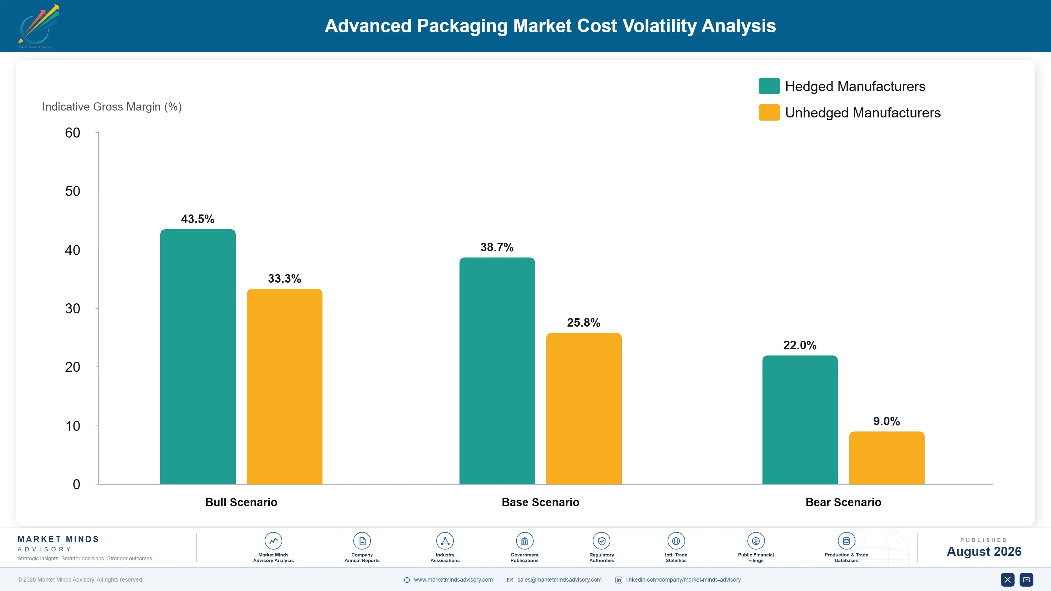
Smaller specialty packaging suppliers carry more exposure than the largest diversified suppliers, since they lack the purchasing scale to negotiate favorable long-term substrate contracts with primary manufacturers. Suppliers sourcing silicon interposers from a concentrated set of foundries face additional exposure to capacity allocation decisions, while those with secured foundry relationships absorb volatility more predictably across their broader global supply chain.
advanced-packaging-market-cost-volatility-analysis-1787301106068

Lock Substrate Pricing Through Annual Contracts

Organic substrates are the largest single volatile input across most advanced package product lines and increasingly competed for by expanding package size requirements. Annual supply agreements with fixed or collared pricing, common practice among larger diversified suppliers, smooth quarter-to-quarter volatility and let commercial teams quote customer contracts with genuine confidence rather than repricing constantly against spot markets.

Diversify Interposer Foundry Sourcing Relationships

Reliance on a single interposer foundry concentrates both price and availability risk unnecessarily across an entire advanced package product line. Qualifying secondary foundry relationships across multiple regions, even at modestly higher unit cost, protects continuity when any single foundry faces capacity allocation pressure or a sudden demand spike from competing accelerator programs industry-wide and across the broader supply base.

Invest in Substrate Manufacturing Capacity Directly

Suppliers that co-invest directly in substrate manufacturing capacity alongside key suppliers secure guaranteed access that pure customers relying on shared allocation cannot match reliably. That direct investment also gives suppliers earlier visibility into capacity timelines, letting them plan product launches with greater confidence than competitors dependent entirely on shared, unsecured spot-market allocation channels alone.

Portfolio Architecture for Margin Defence

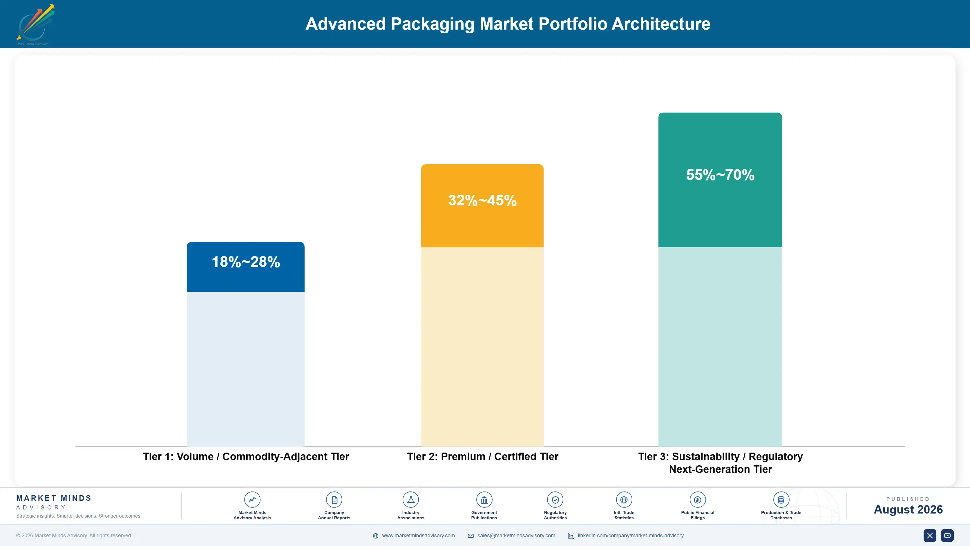
The portfolio splits into three tiers with substantial margin separation tied to process complexity and capacity scarcity. Volume tier products carry mature fan-out and wafer-level packaging, competing largely on price. Premium certified products carry flip chip and system-in-package assemblies backed by documented yield performance. Sustainability and next-generation products, meaning 2.5D interposer and 3D stacked packaging for AI accelerators, attract the sector's most active research investm
The tension between volume and premium runs through nearly every supplier's product roadmap. Volume products fund the manufacturing scale and customer relationships premium products eventually depend on, yet volume margins keep compressing as regional assembly houses scale aggressively on conventional formats. Suppliers that under-invest in premium interposer capability risk missing the single largest profit pool in the industry, while those chasing premium exclusively struggle to fund the manufacturing base for broader consumer electronics demand.

High-value margin pools concentrate overwhelmingly in 2.5D and 3D packaging for AI accelerators where capacity scarcity and technical complexity carry the largest financial stakes, and where documented yield commands extraordinary pricing power. Conventional mobile and consumer packaging generates meaningful steady volume but thinner margin, since that segment competes against lower-cost regional suppliers with adequate but unremarkable process capability.

Volume / Commodity-Adjacent Tier

Mature fan-out and wafer-level packaging for conventional mobile and consumer applications, competing largely on price against a crowded field of regional assembly houses offering broadly comparable process capability and quality across the industry.
Gross Margin: 18-28%

Premium / Certified Tier

Flip chip and system-in-package assemblies backed by documented yield performance and formal customer qualification, commanding meaningful pricing premiums over conventional equivalents across most enterprise server, networking, and high-performance computing markets globally.
Gross Margin: 32-45%

Sustainability / Regulatory / Next-Generation Tier

2.5D interposer and 3D stacked packaging for AI accelerators still severely capacity-constrained across the industry, targeting performance conventional packaging formats simply cannot achieve at any comparable price point or manufacturing scale.
Gross Margin: 55-70%
advanced-packaging-market-portfolio-architecture-1787301106568

High-value Sub-segments and Strategic Watch-out

2.5D Interposer AI Accelerator Packaging

High value and high growth, driven by hyperscaler and sovereign AI infrastructure buildout simultaneously, with capacity and technical barriers protecting incumbent suppliers from new entrant price competition on the largest hyperscaler and sovereign accounts worldwide and their multi-year infrastructure commitments spanning several successive product generations and years.
Gross Margin: 55-70%

Flip Chip Enterprise and Server Packaging

High value with moderate growth, anchored by enterprise server and networking equipment demand, where documented reliability and thermal performance increasingly decide vendor qualification for large corporate procurement contracts across enterprise computing, networking, and data center sectors broadly across every major regional market and customer segment.
Gross Margin: 32-45%

Mobile and Consumer Fan-Out Packaging

The category's largest volume base by unit count, competing on price against a crowded field of regional suppliers, generating steady but thin margin as mobile device packaging demand matures across most developed and rapidly emerging consumer electronics markets worldwide, from flagship smartphones to entry-level wearable devices.
Gross Margin: 18-28%

Legacy Wire-Bond Packaging Formats

Strategic watch-out where advanced flip chip and fan-out formats increasingly threaten to displace legacy wire-bond packaging across most applications, creating genuine technology risk for suppliers slow to transition capacity toward more advanced formats before losing meaningful market share to more technically capable and better-resourced rivals over time.
Gross Margin: 12-20%

Allocation Cycle Economics of Assembly

Packaging demand behaves like an annuity once a customer commits to a specific assembly partner's process, since chip designs are engineered around a particular interposer geometry and switching suppliers requires costly redesign that most customers avoid without a decisive reason. That structure rewards incumbency heavily: a supplier that wins the initial design-in keeps the customer relationship through multiple product generations unless a competitor demonstrates an overwhelming capacity or c
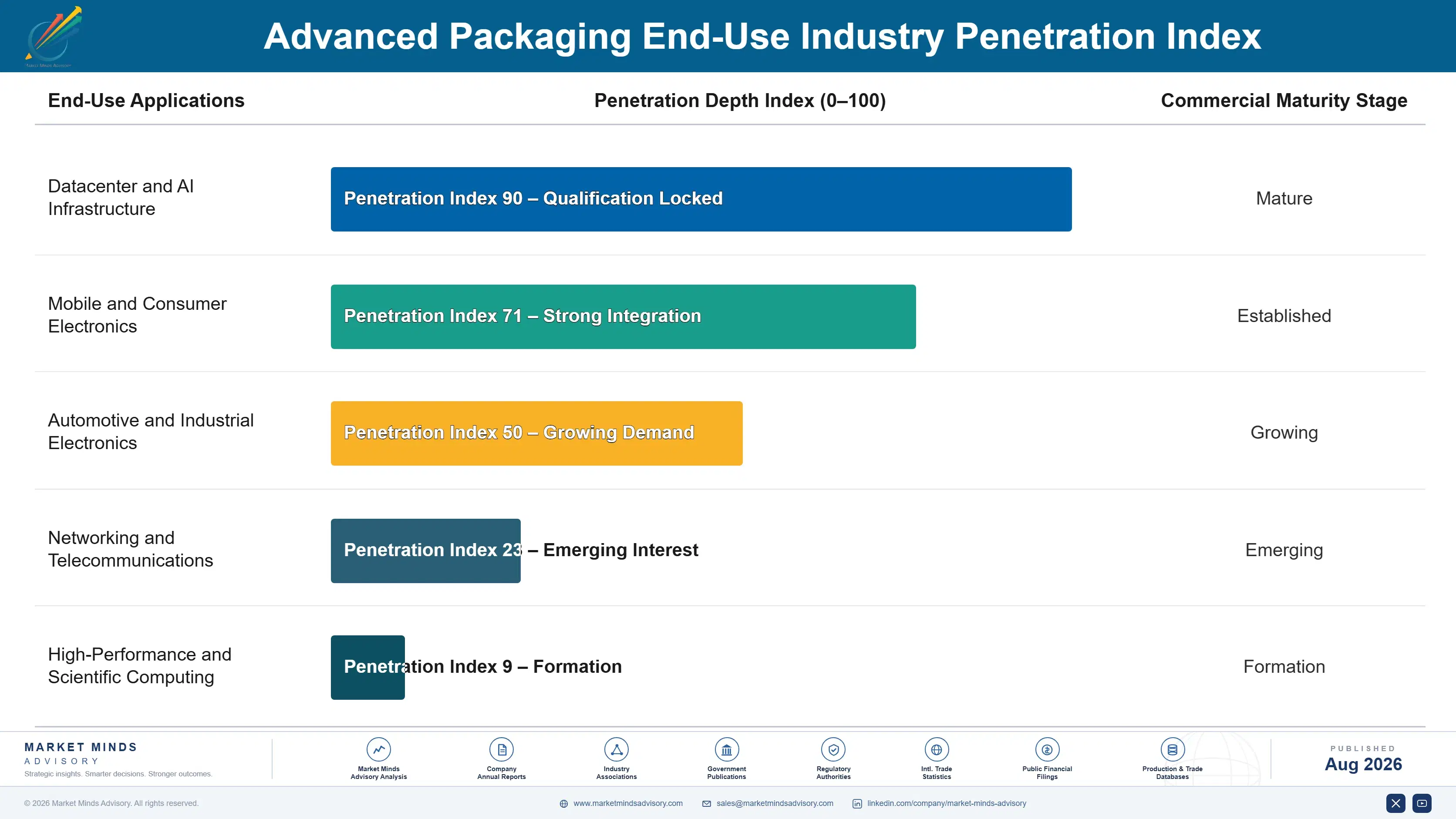
Adoption depth varies sharply by end-use vertical. AI accelerator and high-performance computing customers have adopted the most advanced interposer packaging almost immediately upon availability, since compute density there translates directly into competitive product capability. Mobile and consumer electronics customers lag well behind, treating advanced packaging as aspirational rather than standard, partly because cost sensitivity is genuinely tighter and partly because performance requirements rarely justify premium assembly.

Buyer profiles have shifted generationally. Procurement decisions that once sat primarily with individual design engineers now route through centralized supply chain and capacity planning committees at larger organizations, rewarding suppliers able to present integrated multi-year capacity roadmaps rather than relationship selling alone. Younger chip architects entering leadership roles treat packaging co-design as a core engineering discipline rather than a downstream assembly afterthought.
advanced-packaging-market-end-use-penetration-index-1787301107057

MMA's Read on Advanced Assembly

These are among the four positions where our research anticipates prominent divergence between winners and laggards over the coming forecast period. Each is grounded in the demand model, the regulatory perimeter, and the announced capacity pipeline.
01 / CAPACITY PRE-COMMITMENT STRATEGY

Early allocation lock-in will separate winners from spot-market buyers

Advanced packaging capacity remains severely constrained relative to AI accelerator demand, which means customers relying on spot-market purchasing rather than multi-year pre-commitments will keep facing allocation shortfalls that undermine their own product roadmaps regardless of design quality. Suppliers offering guaranteed capacity through structured long-term agreements address the exact uncertainty that keeps customers awake, a problem raw technical capability alone cannot solve. Those securing pre-commitments now, before capacity constraints ease industry-wide, will lock in customer relationships competitors cannot easily dislodge for years.
02 / YIELD DOCUMENTATION INVESTMENT

Proven track records will define share gains through 2036

Customers increasingly demand documented yield performance before committing expensive dies to a given assembly process, and completing that documentation takes years of production history that cannot be compressed once a customer decision deadline approaches. Suppliers without proven yield records increasingly lose qualification for the highest-value multi-die assemblies, regardless of reputation built in simpler packaging categories over decades. Those investing in documentation and process maturity now, ahead of competitors still building comparable track records, will capture disproportionate share as customers keep raising qualification standards.
03 / FOUNDRY CO-LOCATION POSITIONING

Integrated manufacturing proximity will decide who wins the fastest cycles

Customers racing to bring new AI accelerator products to market increasingly favor packaging partners co-located with leading foundry operations, since the cycle time advantage from eliminating international wafer shipping compounds meaningfully across successive product generations. Suppliers without co-located capacity cannot simply buy their way into this advantage quickly, since building adjacent facilities near major foundry campuses takes years of planning and capital commitment. Incumbent suppliers with existing co-located capacity are positioned to capture a disproportionate share of the fastest-cycle, highest-value customer relationships.
04 / CHIPLET STANDARDIZATION EXPOSURE

Interoperable interconnect standards will permanently reshape competitive positioning

Chiplet interconnect standardization is lowering the barrier for smaller design houses to participate in multi-die architectures, permanently expanding the addressable customer base beyond the handful of companies that once justified building complete in-house packaging expertise. That standardization is simultaneously freeing large assembly houses to serve a broader, more fragmented customer base rather than depending entirely on a small number of hyperscaler relationships for volume. The net effect redraws competitive geography in ways unlikely to reverse regardless of future proprietary interconnect innovation.

Engagement Snapshot From the Field

A live engagement with an industry participant carrying material or product regulatory and market exposure ahead of a defining policy shift, showing how our research translates into a defensible multi-year portfolio strategy.
MARKET MINDS ADVISORY · CLIENT ENGAGEMENT SUMMARY
Advanced Packaging Producer Strategic Portfolio Review and Transition Roadmap 2026·Investment Scenario on Advanced Packaging Exposure Evaluation 2025-26
CLIENT PROFILE
A venture-backed fabless semiconductor company developing a specialized AI inference accelerator, reporting approximately 60 million dollars in committed pre-production revenue, approached MMA while negotiating advanced packaging supply terms ahead of its first commercial production run scheduled for the following fiscal year across multiple planned product variants and multiple distinct target customer segments (client-reported, unverified by MMA).
STRATEGIC CHALLENGE
Leadership faced pressure to secure packaging capacity as a startup competing against much larger, better-capitalized customers for the same constrained interposer allocation across the industry's leading suppliers. Engineering wanted the most technically capable partner regardless of relationship depth, while the board needed assurance that committed production timelines would not slip due to capacity access issues beyond the company's direct control.
MMA APPROACH
MMA benchmarked packaging supplier capacity commitments and allocation practices across the top five suppliers, assessed which suppliers historically prioritized smaller customers versus reserving capacity exclusively for their largest hyperscaler accounts, and modeled realistic allocation timelines under different negotiating, pre-payment, and multi-supplier diversification strategies realistically available to a company of the client's size and stage.
KEY FINDINGS
  1. Suppliers varied considerably in their willingness to allocate meaningful capacity to smaller customers, with two of five candidates offering realistic paths to timely allocation.
  2. Pre-payment commitments meaningfully improved allocation priority even for smaller customers, though the required capital commitment exceeded what the client had initially budgeted.
  3. A secondary, less capacity-constrained supplier offered a viable fallback path despite somewhat lower peak performance specifications and interconnect bandwidth (client-reported, unverified by MMA).
  4. Building a relationship with a smaller regional assembly house alongside the primary supplier provided meaningful negotiating leverage without requiring full capacity diversification.
CLIENT PROFILE
A venture-backed fabless semiconductor company developing a specialized AI inference accelerator, reporting approximately 60 million dollars in committed pre-production revenue, approached MMA while negotiating advanced packaging supply terms ahead of its first commercial production run scheduled for the following fiscal year across multiple planned product variants and multiple distinct target customer segments (client-reported, unverified by MMA).
STRATEGIC CHALLENGE
Leadership faced pressure to secure packaging capacity as a startup competing against much larger, better-capitalized customers for the same constrained interposer allocation across the industry's leading suppliers. Engineering wanted the most technically capable partner regardless of relationship depth, while the board needed assurance that committed production timelines would not slip due to capacity access issues beyond the company's direct control.
MMA APPROACH
MMA benchmarked packaging supplier capacity commitments and allocation practices across the top five suppliers, assessed which suppliers historically prioritized smaller customers versus reserving capacity exclusively for their largest hyperscaler accounts, and modeled realistic allocation timelines under different negotiating, pre-payment, and multi-supplier diversification strategies realistically available to a company of the client's size and stage.
KEY FINDINGS
  1. Suppliers varied considerably in their willingness to allocate meaningful capacity to smaller customers, with two of five candidates offering realistic paths to timely allocation.
  2. Pre-payment commitments meaningfully improved allocation priority even for smaller customers, though the required capital commitment exceeded what the client had initially budgeted.
  3. A secondary, less capacity-constrained supplier offered a viable fallback path despite somewhat lower peak performance specifications and interconnect bandwidth (client-reported, unverified by MMA).
  4. Building a relationship with a smaller regional assembly house alongside the primary supplier provided meaningful negotiating leverage without requiring full capacity diversification.
RECOMMENDED STRATEGY
Phase 1: Phase 1 (0 to 6 months): Secure a pre-payment allocation commitment with the most capacity-accessible top-tier supplier identified in the analysis. Phase 2: Phase 2 (6 to 12 months): Qualify a secondary regional assembly house as a fallback option, preserving negotiating leverage at the primary supplier. Phase 3: Phase 3 (12 to 24 months): Reassess supplier strategy as production volume scales and the company's negotiating position strengthens with proven revenue.
OUTCOME
The startup secured allocation commitments sufficient to support its planned production timeline without the delays initially feared, and the secondary supplier relationship has since provided useful negotiating leverage during subsequent capacity renewal discussions and helped the company avoid a costly production delay entirely (client-reported, unverified by MMA).

Frequently Asked Questions

Foundational context covering the market sizes, CAGR, scope, country, region and competition that inform every finding below. This section is provided to cover basics and most often pre-purchase conversations, answered from the MMA Primary Research Dataset.

What is the current size of the Advanced Packaging Market?

The market reached an estimated 48.0 billion dollars in 2025. That figure reflects global revenue across 2.5D interposer, 3D stacked die, fan-out, flip chip, system-in-package, and wafer-level chip-scale packaging.

How large will the Advanced Packaging Market be by 2036?

MMA projects the market will reach approximately 148.3 billion dollars by 2036 under the base case scenario. That represents roughly 2.79 times the 2026 market value.

What is the CAGR for the Advanced Packaging Market 2026 to 2036?

The base case CAGR is 10.8% annually across the full ten-year forecast period. Bull and bear scenarios run 12.1% and 9.5% respectively, reflecting capacity expansion timing uncertainty.

Which segment is growing fastest?

2.5D and interposer packaging grows fastest at 18.5% CAGR, about 1.71 times the overall market rate. AI accelerator integration of compute and memory dies is the primary driver.

Who are the major companies in the Advanced Packaging Market?

TSMC, ASE Technology, Amkor, Samsung, and Intel lead the category by a consistent revenue basis. Together they hold roughly 64% of global advanced packaging revenue.

Which country is growing fastest?

South Korea leads national growth at an estimated 13.8% CAGR, driven by Samsung and SK Hynix scaling high-bandwidth memory and 3D stacking capacity. AI accelerator demand keeps intensifying.

Report Segmentation Architecture

The full report scope spans multiple orthogonal segmentation dimensions, with cross-tabulated demand data provided for each dimension pair. Coverage extends further to regional breakdowns, trend trajectories, and the competitive detail needed to support segment-level decision-making.

By Packaging Technology Type

  • 2.5D and Interposer Packaging
  • 3D Stacked Die Packaging
  • Fan-Out Wafer-Level Packaging
  • Flip Chip Packaging
  • System-in-Package
  • Wafer-Level Chip-Scale Packaging

By End-Use Industry

  • Datacenter and AI Infrastructure
  • Mobile and Consumer Electronics
  • Automotive and Industrial Electronics
  • Networking and Telecommunications
  • High-Performance and Scientific Computing

By Commercial Dimension

  • Direct Fabless Contract Sales
  • Foundry-Integrated Turnkey Services
  • Custom Interposer Design Partnerships
  • Distributor and OSAT Channel Sales

By Region

  • North America
  • Western Europe
  • East Asia
  • South Asia and Pacific
  • Latin America
  • Middle East and Africa
  • Eastern Europe

Scope, Methodology, and Coverage

Every figure in this report is reproducible from documented input assumptions. The scope below maps the historical period, the forecast horizon, the segmentation dimensions, and the countries covered, alongside the underlying primary and qualitative methodology.
Historical Period
2020 to 2025
Forecast Period
2026 to 2036
Base Year
2025 (USD billions; MMA Primary Research Dataset, August 2026)
Market Definition
The advanced packaging market covers 2.5D interposer, 3D stacked die, fan-out wafer-level, flip chip, system-in-package, and wafer-level chip-scale packaging technologies used to assemble semiconductor dies into finished chip products. It includes assembly services, associated materials, and custom interposer design partnerships. Wafer fabrication, standalone testing services unrelated to packaging, and simple wire-bond assembly for basic consumer electronics are excluded.
Quantitative Units
USD billions (current prices); unit shipment volume where applicable
Segmentation Dimensions
By Packaging Technology Type; By End-Use Industry; By Commercial Dimension; By Region
Regions Covered
North America, Western Europe, East Asia, South Asia and Pacific, Latin America, Middle East and Africa, Eastern Europe
Countries Covered
USA, China, Germany, France, UK, Japan, South Korea, India, Australia, Canada, Brazil, Mexico, Indonesia, Vietnam, Thailand, Malaysia, UAE, Saudi Arabia, South Africa, Nigeria, Turkey, Poland, Netherlands, Italy, Spain, Sweden, Switzerland, Argentina, Colombia, Singapore, and additional markets relevant to this sector
Key Companies Profiled
Taiwan Semiconductor Manufacturing Company Limited; ASE Technology Holding Co., Ltd.; Amkor Technology, Inc.; Samsung Electronics Co., Ltd.; Intel Corporation; JCET Group Co., Ltd.; Powertech Technology Inc.; Tongfu Microelectronics Co., Ltd.; Deca Technologies Inc.; Applied Materials, Inc.; ASM International N.V.; BE Semiconductor Industries N.V.; Kulicke & Soffa Industries, Inc.; Shinko Electric Industries Co., Ltd.; Ibiden Co., Ltd.; Unimicron Technology Corp.; Nepes Corporation; Chipbond Technology Corporation; King Yuan Electronics Co., Ltd.; GlobalFoundries Inc.
Quantitative Methodology
Primary survey, n=3,800 respondents, Q4 2025, six countries; demand-side model with trade association cross-validation
Qualitative Methodology
47 expert interviews, Q4 2025; applied to validate demand model assumptions, identify emerging dynamics, and assess competitive positioning
Report Format
PDF and XLSX data workbook (Word format preview document)
Publisher
Market Minds Advisory
Report Code
MMA-2026-TEC-202
Published
August 2026
Contact
sales@marketmindsadvisory.com | www.marketmindsadvisory.com

Purchase the full Advanced Packaging Market Report (2026 to 2036).

The full MMA Advanced Packaging report sizes the market across six technology categories, five end-use industries, four commercial contracting models, and seven regions through 2036. It profiles twenty participants on a consistent basis of packaging revenue, scoring the top five on capacity scale, yield documentation, and foundry co-location depth. Scenario models quantify how AI accelerator design complexity, chiplet standardization, and substrate price volatility move both demand and achievable pricing. The report also includes delivered cost modeling by technology category, a capacity expansion tracker across major suppliers, and a supplier displacement risk assessment built for fabless designers, assembly houses, and investors.
Six-segment technology demand model through 2036
Capacity expansion and allocation tracker across suppliers
Yield documentation competitive positioning assessment tool
Foundry co-location benchmarking dataset and analysis
Substrate and interposer cost sensitivity model
Supplier displacement risk scoring by technology

Built For The People Who Decide

From boardroom strategy to bench-side execution, this report is read cover-to-cover by leaders shaping the next decade of their industry, turning demand scenarios, market dynamics and valuation benchmarks into decisions.
CXOs/ Presidents/ VPs/ Managers
M&A and Corporate Development
Strategy Teams and R&D Heads
Procurement and Product Directors
Regulatory and Compliance Leaders
Investor Relations and Equity Analysts